Key Findings: Advantest, in mixed-signal SoC design, sees 50X speedup, 25 day test reduced to 12 hours, dramatic test coverage increase.
Trolling through the CDNLive archives, I discovered another gem. At the May 2013 CDNLive in Munich, Thomas Henkel and Henriette Ossoinig of Advantest presented a paper titled “Timing-accurate emulation of a mixed-signal SoC using Palladium XP”. Advantest makes advanced electronics test equipment. Among the semiconductor designs they create for these products is a test processor chip with over 100 million logic transistors, but also with lots of analog functions.They set out to find a way to speed up their full-chip simulations to a point where they could run the system software. To do that, they needed about a 50X speed-up. Well, they did it!
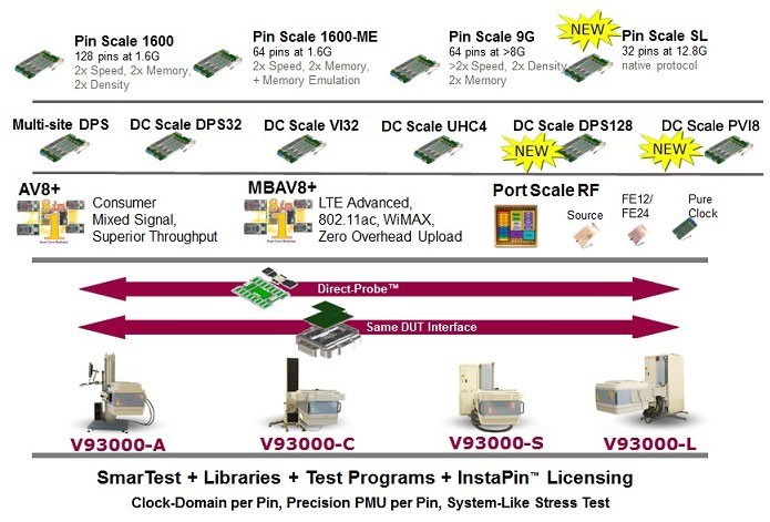
Figure 1: Advantest SoC Test Products
To skip the commentary, read Advantest's paper here.
Problem Statement
Software is becoming a bigger part of just about every hardware product in every market today, and that includes the semiconductor test market. To achieve high product quality in the shortest amount of time, the hardware and software components need to be verified together as early in the design cycle as possible. However, the throughput of a typical software RTL simulation is not sufficient to run significant amounts of software on a design with hundreds of millions of transistors.
Executing software on RTL models of the hardware means long runs (“deep cycles”) that are a great fit for an emulator, but the mixed-signal content posed a new type of challenge for the Advantest team. Emulators are designed to run digital logic. Analog is really outside of the expected use model. The Advantest team examined the pros and cons of various co-simulation and acceleration flows intended for mixed signal and did not feel that they could possibly get the performance they needed to have practical runtimes with software testbenches. They became determined to find a way to apply their Palladium XP platform to the problem.
Armed with the knowledge of the essential relationship between the analog operations and the logic and software operations, the team was able to craft models of the analog blocks using reduction techniques that accurately depicted the essence of the analog function required for hardware-software verification without the expense of a continuous time simulation engine.
The requirements boiled down to the following:
• Generation of digital signals with highly accurate and flexible timing
• Complete chip needs to run on Palladium XP platform
• Create high-resolution timing (100fs) with reasonable emulation performance, i.e. at least 50X faster than simulation on the fastest workstations
Solution Idea
The solution approach chosen was to simplify the functional model of the analog elements of the design down to generation of digital signal edges with high timing accuracy. The solution employed a fixed-frequency central clock that was used as a reference.Timing-critical analog signals used to produce accurately placed digital outputs were encoded into multi-bit representations that modeled the transition and timing behavior. A cell library was created that took the encoded signals and converted them to desired “regular signals”.
Automation was added to the process by changing the netlisting to widen the analog signals according to user-specified schematic annotations. All of this was done in a fashion that is compatible with debugging in Cadence’s Simvision tool. Details on all of these facets to follow.
The Timing Description Unit (TDU) Format
The innovative thinking that enabled the use of Palladium XP was the idea of combining a reference clock and quantized signal encoding to create offsets from the reference. The implementation of these ideas was done in a general manner so that different bit widths could easily be used to control the quantization accuracy.
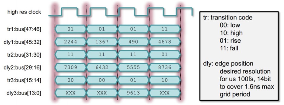
Figure 2: Quantization method using signal encoding
Timed Cell Modeling
You might be thinking – timing and emulation, together..!? Yes, and here’s a method to do it….
The engineering work in realizing the TDU idea involved the creation of a library of cells that could be used to compose the functions that convert the encoded signal into the “real signals” (timing-accurate digital output signals). Beyond some basic logic cells (e.g., INV, AND, OR, MUX, DFF, TFF, LATCH), some special cells such as window-latch, phase-detect, vernier-delay-line, and clock-generator were created. The converter functions were all composed from these basic cells. This approach ensured an easy path from design into emulation.
The solution was made parameterizable to handle varying needs for accuracy. Single bit inputs need to be translated into transitions at offset zero or a high or low coding depending on the previous state. Single bit outputs deliver the final state of the high-resolution output either at time zero, the next falling, or the next rising edge of the grid clock, selectable by parameter. Output transitions can optionally be filtered to conform to a configurable minimum pulse width.
Timed Cell Structure
There are four critical elements to the design of the conversion function blocks (time cells):
Input conditioning – convert to zero-offset, optional glitch preservation, and multi-cycle path
Transition sorting – sort transitions according to timing offset and specified precedence
Function – for each input transition, create appropriate output transition
Output filtering – Capability to optionally remove multiple transitions, zero-width, pulses, etc.
Timed Cell Caveat
All of the cells are combinational and deliver a result in the same cycle of an input transition. This holds for storage elements as well. For example a DFF will have a feedback to hold its state. Because feedback creates combinational loops, the loops need a designation to be broken (using a brk input conditioning function in this case – more on this later). This creates an additional requirement for flip-flop clock signals to be restricted to two edges per reference clock cycle.
Note that without minimum width filtering, the number of output transitions of logic gates is the sum of all input transitions (potentially lots of switching activity). Also note that the delay cell has the effect of doubling the number of output transitions per input transition.
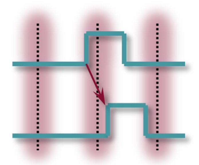
Figure 3: Edge doubling will increase switching during execution
SimVision Debug Support
The debug process was set up to revolve around VCD file processing and directed and viewed within the SimVision debug tool. In order to understand what is going on from a functional standpoint, the raw simulation output processes the encoded signals so that they appear as high-precision timing signals in the waveform viewer. The flow is shown in the figure below.
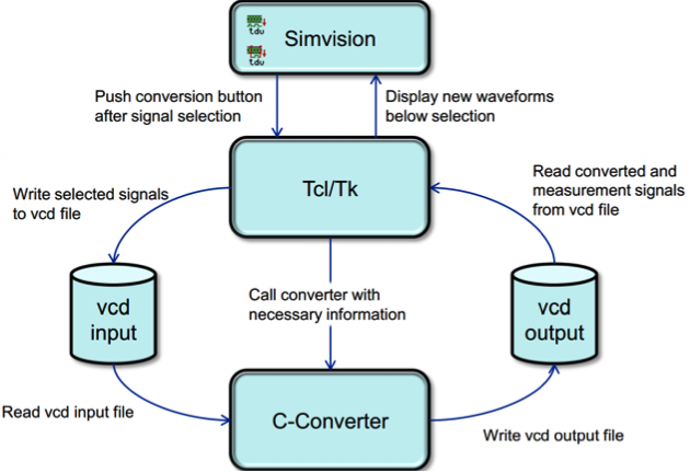
Figure 4: Waveform post-processing flow
The result is the flow is a functional debug view that includes association across representations of the design and testbench, including those high-precision timing signals.
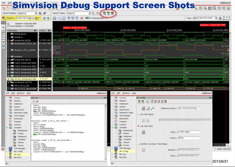
Figure 5: Simvision debug window setup
Overview of the Design Under Verification (DUV)
Verification has to prove that analog design works correctly together with the digital part. The critical elements to verify include:
• Programmable delay lines move data edges with sub-ps resolution
• PLL generates clocks with wide range of programmable frequency
• High-speed data stream at output of analog is correct
These goals can be achieved only if parts of the analog design are represented with fine resolution timing.

Figure 6: Mixed-signal design partitioning for verification
How to Get to a Verilog Model of the Analog Design
There was an existing Verilog cell library with basic building blocks that included:
- Gates, flip-flops, muxes, latches
- Behavioral models of programmable delay elements, PLL, loop filter, phase detector
With a traditional simulation approach, a cell-based netlist of the analog schematic is created. This netlist is integrated with the Verilog description of the digital design and can be simulated with a normal workstation. To use Palladium simulation, the (non-synthesizable) portions of the analog design that require fine resolution timing have to be replaced by digital timing representation. This modeling task is completed by using a combination of the existing Verilog cell library and the newly developed timed cells.
Loop Breaking
One of the chief characteristics of the timed cells is that they contain only combinational cells that propagate logic from inputs to outputs. Any feedback from a cell’s transitive fanout back to an input creates a combinational loop that must be broken to reach a steady state. Although the Palladium XP loop breaking algorithm works correctly, the timed cells provided a unique challenge that led to unpredictable results. Thus, a process was developed to ensure predictable loop breaking behavior. The user input to the process was to provide a property at the loop origin that the netlister recognized and translated to the appropriate loop breaking directives.
Augmented Netlisting
Ease of use and flow automation were two primary considerations in creating a solution that could be deployed more broadly. That made creating a one-step netlisting process a high-value item. The signal point annotation and automatic hierarchy expansion of the “digital timing” parameter helped achieve that goal. The netlister was enriched to identify the key schematic annotations at any point in the hierarchy, including bit and bus signals.
Consistency checking and annotation reporting created a log useful in debugging and evolving the solution.
Wrapper Cell Modeling and Verification
The netlister generates a list of schematic instances at the designated “netlister stop level” for each instance the requires a Verilog model with fine resolution timing. For the design in this paper there were 160 such instances.
The library of timed cells was created; these cells were actually “wrapper” cells comprised of the primitives for timed cell modeling described above. A new verification flow was created that used the behavior of the primitive cells as a reference for the expected behavior of the composed cells. The testing of the composed cells included had the timing width parameter set to 1 to enable direct comparison to the primitive cells. The Cadence Incisive Enterprise Simullator tool was successfully employed to perform assertion-based verification of the composed cells versus the existing primitive cells.
Mapping and Long Paths
Initial experiments showed that inclusion of the fine resolution timed cells into the digital emulation environment would about double the required capacity per run. As previously pointed out, the timed cells having only combinational forward paths creates a loop issue. This fact also had the result of creating some such paths that were more than 5,000 steps of logic. A timed cell optimization process helped to solve this problem. The basic idea was to break the path up by adding flip-flops in strategic locations to reduce combinational path length. The reason that this is important is that the maximum achievable emulation speed is related to combinational path length.
Results
Once the flow was in place, and some realistic test cases were run through it, some further performance tuning opportunities were discovered to additionally reduce runtimes (e.g., Palladium XP tbrun mode was used to gain speed). The reference used for overall speed gains on this solution was versus a purely software-based solution on the highest performance workstation available.
The findings of the performance comparison were startlingly good:
• On Palladium XP, the simulation speed is 50X faster than on Advantest’s fastest workstation
• Software simulation running 25 days can now be run in 12 hours -> realistic runtime enables long-running tests that were not feasible before
• Now have 500 tests that execute once in more than 48 hours
• They can be run much more frequently using randomization and this will increase test coverage dramatically
Steve Carlson
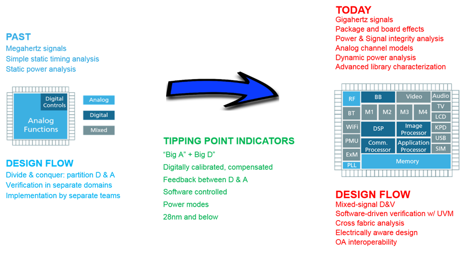
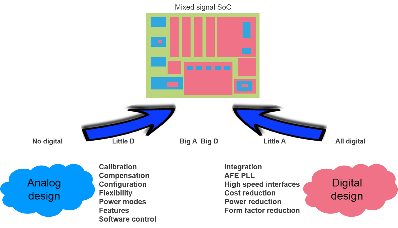


 Analog and Mixed-signal (AMS) designs are increasingly using active power management to minimize power consumption. Typical mixed-signal design uses several power domains and operate in a dozen or more power modes including multiple functional, standby and test modes. To save power, parts of design not active in a mode are shut down or may operate at reduced supply voltage when high performance is not required. These and other low power techniques are applied on both analog and digital parts of the design. Digital designers capture power intent in standard formats like Common Power Format (CPF), IEEE1801 (aka Unified Power Format or UPF) or Liberty and apply it top-down throughout design, verification and implementation flows. Analog parts are often designed bottom-up in schematic without upfront defined power intent. Verifying that low power intent is implemented correctly in mixed-signal design is very challenging. If not discovered early, errors like wrongly connected power nets, missing level shifters or isolations cells can cause costly rework or even silicon re-spin.
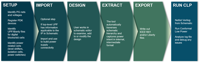
 Virtuoso Power Manager is new tool released in the Virtuoso IC6.1.8 platform which is capable of managing power intent in an Analog/MS design which is captured in Virtuoso Schematic Editor. In setup phase, the user identifies power and ground nets and registers special devices like level shifters and isolation cells. The user has the option to import power intent into IEEE1801 format, applicable for top level or any of the blocks in design. Virtuoso Power Manager uses this information to traverse the schematic and extract complete power intent for the entire design. In the final stage, Virtuoso Power Manager exports the power intent in IEEE1801 format as an input to the formal verification tool (Cadence Conformal-LP) for static verification of power intent.