Quantcast
Channel: Analog/Custom Design (Analog/Custom design)
Viewing all 126 articles
Browse latest View live

Support for Low Power Mixed Signal Designs in Virtuoso Schematic-XL

$
0
0

Why is There a Need for Low Power Solutions?

With an increase in the demand for high-performance, multi-tasking systems-on-chips (SoCs) for communication and computing, the power requirements for these electronic chips have also greatly increased. There has been a surge in the production of portable devices like mobile phones, laptops, tablets, and game boxes that support multiple applications and use various multimedia features extensively. Also, the usage time for these devices has gone up significantly, which also increases the power consumption for the devices.

However, the technology for batteries has not evolved at the same pace, and a common problem facing the designers is the battery life of the device. The battery technology is also not expected to change drastically in the near future due to various technology and safety reasons. This further accentuates the need to support low power devices. There is also a higher demand in the market for devices that provide for a better in-use and stand-by battery life.

Since the size of the designs is also getting smaller, there is a considerable need to optimize the usage of power to prevent unwanted increases in temperature due to the high activity of the power structures. There is a need for techniques that can conserve power to improve the energy efficiency without penalizing the performance of the design. Consequently, designers use various techniques that help in reducing the consumption of power, thereby increasing the battery life of the final product and also achieving a reduction in size of the battery.

The use of Multi Supply Multi Voltage (MSMV) methodology is a very common practice to achieve these objectives. It includes the use of additional circuitry to control the power behavior of the cells in the design. Some of the basic techniques for this methodology include:

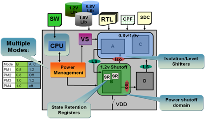
  • Supplying a different set of voltage to different group of cells and thereby creating multiple power domains in the design.
  • Using special low power cells to switch between different power supply levels in the design.
  • Shutting off groups of cells during specific periods of circuit activity, while retaining the value stored, thereby creating different power modes of operation on the same design.
  

A Low Power Design Structure

This new requirement for low power designs provides a very interesting challenge to the EDA industry to address, since the issue is not an isolated tool problem and has an impact across various product lines.

Requirements for a Low Power Mixed-Signal Flow

While the usage of these low power techniques provide a certain benefit to the overall power consumption of the design, it also poses some serious challenges for the automation and support of this methodology, particularly for mixed signal and custom IC designs. Some of the important requirements to create a successful low power mixed-signal flow are:

  • It should be possible to manage the design intent and the power intent separately so that each can be independently optimized during the IP creation.
  • There should be a universally acceptable format/language to describe the power intent that can be deployed across the flow and supported by various EDA vendors
  • It should be possible to package and export the power intent along with the design IP to be used with various tools.
  • The flow should have the ability to automatically extract power intent for complex mixed signal and custom cells. As the design information is captured in schematics and not as a netlist, the power intent is already specified in most of the cases and it is very tedious to traverse the multiple levels of hierarchy to extract this information.
  • It is equally necessary to verify the power description of the design which is automatically extracted by the tool along with the functionality before the IP is integrated in other designs.
  • Also, when the IP is integrated in other designs, one has to make sure that the power intent defined for that instance is available for use in the top design

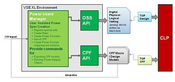
Low Power Mixed-Signal Capabilities in Virtuoso Schematic-XL

Keeping the above requirements in mind, the Virtuoso Schematic-XL suite offers a convenient and highly automated solution that supports the development of complex custom low power mixed-signal designs.

Automated Flow for CPF Extraction and Verification

Macro model and Design CPF extraction from schematics. The power intent for mixed signal and analog blocks is often built into the design, and can be a pretty complex task to describe independently. It often requires the designer to reverse-engineer the design to infer the power intent and capture it accurately. It is a very time consuming and error prone task in the current flows, as the designs can have a large hierarchy with blocks that are implemented by different designers. The new Power Intent Export Assistant (PIEA) in Virtuoso is able to automatically extract the power intent from custom/mixed-signal schematic and export it as a Common Power Format (CPF) specification. The tool is equally adept in extracting both a macro model CPF with the boundary ports to describe the low power interface of the block. It can also extract the full design level CPF for describing the complete power intent of the design.

To use this automatic CPF extraction capability in PIEA, the user just needs to do a one-time quick setup that involves providing the description of the devices, special low power cells and the supply nets. The extraction process is highly automated and manual intervention is minimally required to add and edit the power descriptions. The tool also facilitates the manual entry for the user to specify the power domains, nominal conditions and the power modes. A user can also configure the special library cells such as level shifters, isolation cells and power switches, and also define various rules associated with these cells in the design.


Automatic Extraction of Power Intent by PIEA

Integration of Digital IP blocks. The integration of digital IP blocks with low power specifications in mixed signal designs poses quite a few challenges. Since the block could be working in a different power domain than the other blocks in the design, it is necessary that the power structures required for the block are available in the top level design. This causes different power domains to exist in the design. Designers should make sure that the domain mapping happens correctly from the top to the block so that the correct power signals are propagated across the hierarchy. Also, there is a need to verify that the various special cells like the level shifters and isolation cells are inserted properly across power domain crossings to match with the power requirements of the top level design.

For IP blocks that have an associated CPF specification, Virtuoso Schematics-XL provides a mechanism to import the CPF file, with the power content, and associate it with its schematic or symbol view. The information in the CPF file is then used at the time of extracting the CPF for the top level schematic in which the IP is being integrated. This helps in not only an accurate power intent extraction for the top level, but also in the power verification of the mixed-signal design as the power intent of the digital IP has been captured in the top level CPF.

Verification of power intent. After the CPF file has been extracted, there is a need to verify that the extracted power intent specification is complete and accurately captures the power intent built into the design. To facilitate the verification of the power intent, PIEA provides an interface with the Cadence Conformal Low Power (CLP) tool.

This integration makes the power verification for custom and mixed-signal designs a very easy task. The designer does not have to worry about the generation of inputs for the CLP tool. The mixed-signal design is written out as a digital netlist with the analog cells marked as black boxes. The interface also automatically creates the run files for the CLP tool. CLP is launched in the background automatically and the CLP output window is brought up for the user to analyze the results. This verification can be done both at the chip or block level for the power intent.


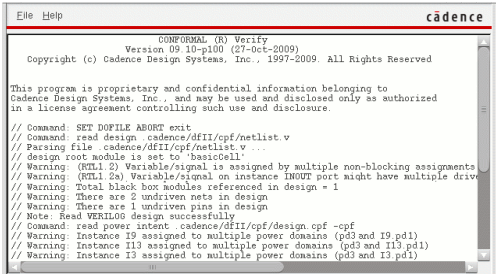
The CLP output window after the verification of extracted CPF

CPF import support for CDL Generation for LVS Verification. Since not all physical verification tools support Verilog and CPF as the input for layout-versus-schematic (LVS), it becomes necessary in the physical verification flow to create a CDL file for the digital blocks. The traditional methods have a limitation on the usage of both the logical and the physical Verilog for a complete schematic generation. Importing a logical Verilog file without the CPF results in a schematic with no power and ground connections, since there is no power description in the logical Verilog netlist. Similarly the import of physical Verilog requires that the standard cell libraries within Virtuoso have explicit PG terminals. This is not always possible, as most designers use the inherited connections to propagate the power and ground connections. But with the CPF import support in Virtuoso, it becomes easy to read in the logical Verilog and annotate the power intent from the CPF on to the schematic created. This creates the correct power and ground net information in the schematic to enable the export of CDL for the LVS verification.

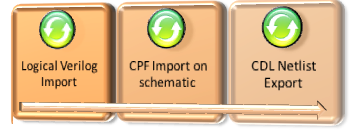
CDL Generation flow for Digital Designs

Design portability and reuse. With all the features to support the read and write of CPF in the Virtuoso Schematics-XL suite, it can be used as a common ASCII format for low power description reusable across all tools. The same digital cell CPF used during the synthesis and physical implementation can be used for the top level CPF extraction in Virtuoso, where the digital block is instantiated. It can also be used to aid in the creation of CDL when the digital block has to be verified for LVS. The macro model CPF generated for analog designs can be used when these analog designs are instantiated in the digital world.

Concluding Remarks

The generation of CPF manually has long been a very time consuming and error prone task for mixed signal and custom designs. The capabilities in Virtuoso Schematics-XL provide a lot of productivity improvement for the low power flow. Also, the integration with Conformal makes sure that the CPF file content is accurate, complete and usable. These features, along with the support for CPF import, facilitate the ease of design portability and IP integration for capturing power intent.


How Can You Learn About Mixed-Signal Verification and Implementation Flows at Your Desk?

$
0
0

The vast majority of SoCs today are advanced mixed-signal designs. The old mixed-signal world looked like an analog environment on the left bolted to a digital environment on the right. Depending on which engineering group was responsible for final assembly, one part would be treated as a black box and the two parts would be bolted together at the system-on-chip (SoC) level. But today's mixed-signal designs have multiple feedback loops, complex modeling requirements, and higher performance targets. This means it's no longer possible to deconstruct designs into separate analog and digital functions. Engineers must embrace the digital-centric metric-driven verification methodologies into their mixed-signal verification (MSV) flows. Engineers also need an integrated MSV environment that focuses on performance and reliability. Top-level SoC verification has become a critical challenge-and functional failures can result in costly design iterations and missed market windows.

Success demands that tool, methodologies, and design teams rethink and break out of traditional silos in various functional and technology disciplines, and collaborates across the design chain and ecosystem. Cadence has had the opportunity to team with the world's top semiconductor companies and ecosystem partners on every significant mixed-signal design over the past 25 years, and has thus evolved its MSV solutions to address this demand. Mixed-signal simulators and environments such as Cadence's Virtuoso® AMS Designer Simulator and Incisive® simulators have evolved to support true mixed-signal simulations.


Furthermore, by interfacing the Virtuoso and Encounter platforms through the industry-standard OpenAccess (OA) database, Cadence has also enabled a new generation of interoperable mixed-signal flows and methodologies that help analog and digital design teams efficiently implement complex mixed-signal designs. This has resulted in fewer iterations and communication errors between design teams, especially during floorplanning, chip integration, and engineering change order (ECO) processes.

So, I'll now ask, "Are you interested in learning various aspects of mixed-signal verification and implementation flows, provided by Cadence, with a do-it-yourself (DIY) approach?"

  • Modeling analog circuits with WREAL
  • Introduction to AMS Designer Simulation
  • Mixed-Signal Low-Power Structural Verification
  • Digital Mixed-Signal (DMS) Implementation using EDI and Virtuoso
  • CPF-AMS Low-Power Mixed-Signal Simulation
  • Schematic Model Generator
  • amsDmv - AMS Design and Model Validation
  • Analog-on-Top Mixed-Signal Implementation: Virtuoso Black Box Flow with IC61
  • Mixed-Signal Simulation with Real Number Modeling
  • Mixed-Signal Verification - Connectivity
  • Mixed-Signal Verification - System Verilog Real Number Modeling

Rapid Adoption Kits (RAKs) from Cadence help engineers learn foundational aspects of Cadence tools and design and verification methodologies using a "DIY" approach. The associated application notes, tutorials and videos also aid to develop a deep understanding of the said subject. Please don't get me wrong: instructor-led, structured training programs work beautifully if you can invest the time and money. But there is always demand for learning something simply and quickly on your own in some corner of the world. 

Today, we have eleven (11) RAKs, on subjects mentioned in the above list that are focused to help our users learn various aspects of mixed-signal verification and implementation flows.They demonstrate how you can improve your productivity and maximize the benefits of Cadence tools and technologies in the mixed-signal space.

These RAKs are an outstanding resource for both new and experienced circuit designers to understand the many facets of mixed-signal design, verification, and implementation. The many examples provided in the labs, along with provided example code, make these RAKs a must-do for anyone involved in the day-to-day design of mixed-signal systems.

Download your mixed-signal RAK today from htttp://support.cadence.com/ms-raks

The big challenge that I have faced with learning is how to find the right learning vehicle that helps me discover what I didn't already know in a short period of time. If you also struggle with this, be sure to look into our RAKs, available at http://support.cadence.com/raks

Please note that you will need your Cadence customer credentials to logon to Cadence Online Support http://support.cadence.com, your 24/7 partner for getting help in resolving issues related to Cadence software or learning Cadence tools and technologies.

Happy Learning!

Sumeet Aggarwal

It’s Late, But the Party is Just Getting Started

$
0
0

Key Findings: Many more chip programs are crossing the tipping point and need advanced mixed-signal verification methodologies and technologies. A deterministic march to closure is needed.  The Cadence party for mixed-signal verification is the hottest ticket in town.

With some important public events now behind us and more on the horizon, the agendas make it clear that there is mounting pain in the realm of verifying chips with a significant blend of analog and digital circuitry. While this is not news to those in the know, it is fresh pain for a growing legion of SoC verification teams. It is starting to look as though the industry may be ready to cross the proverbial chasm if the topics at these events are reliable indicators. And the good news is that there has been a mixed-signal verification party going on for more than 20 years at Cadence, and for all of the newcomers, we’d like to welcome you!

What’s driving party attendance?

Back in 2009, some really good work was done, probably about five years ahead of its time. This was when the seminal work on applying the industry’s best practices on digital SoC verification was applied to the mixed-signal SoC verification problem. But, before diving into the particulars, let’s review the driving forces. 

At the speed of Moore’s Law, two worlds are colliding. Advanced nodes (28nm and below) have been key drivers in the evolution of analog design with needs for digital compensation and calibration on a steep rise.  Massive integration capability of digital SoCs has led to the inclusion of more, and more complex, analog IP blocks. So whether you started from the “analog side” or the “digital side,” chances are you now have to be a lot more cognizant that it is a blended world and act accordingly.

mixed-signal SoC implementation

Figure 1: Drivers of advanced mixed-signal verification methodologies

Figure 1 shows how complexity comes from all over the place, and that complexity creates challenges that rapidly transform into critical business issues. Left unchecked, these issues are pretty bad news. What I hear consistently is that there has been more bad news. But, sometimes, bad news is the impetus to drive change, and that can be a great thing.

When we talk about the industry best practices in mixed-signal SoC verification, we are, of course, talking about a host of elements that include technologies, capabilities, and methodologies. But let's not overlook the value of experience.

I am going to “limit” the scope to mixed-signal simulation technology and methodology. What we have proven in terms of formal, static, and other areas can be covered in coming posts (cheers).

So, the party is raging and everyone is having a great time, but they are all dancing around that big elephant right in the middle of the room. For mixed-signal verification, that elephant is named modeling. More about that in my installment of The Low Road.

Critical elements for a good party

Back to the party. Just like a great party has to have fun people, good food, and great music, there is a lot that goes into a great mixed-signal simulation solution. Starting with the basic needs perspective, the crucial elements are:

  • Approach: There are industry best practices that have been applied on the biggest, most complex digital SoCs ever created. It turns out that the overhead of the structure and rigor of this approach is not so large as to only apply to billion transistor digital designs. The approach is practical, thorough, and proven. It is the Metrics-driven Unified Verification Methodology for Mixed-Signal SoC--affectionately known from here on out as MD-UVM-MS (and yes, there will be a more acronyms).  What is special here is the adaptation of the special needs of analog designers.  
  • Methodology: Having a methodology that scales provides uniformity, and reuse is at the core of the value proposition for the Unified Verification Methodology (UVM). The standard creates an object-oriented modular approach that can be parameterized.  There are lots of great documentation and training resources available on UVM (see, for instance, this UVM primer and this UVM backgrounder).
  • Measure: The old adage, 'what you measure will improve' certainly has been proven for SoC verification. There are many metric types that are being used today for measuring the progress, effectiveness, and completeness of an SoC verification suite. Further, the linking of the metrics to tests and then to the debug environment creates a much faster, more methodical, path to verification convergence. Click here for more information.
  • Leverage multi-engine technology: Just like a general-purpose processor is great to have in an SoC and you may also find many other computational elements on the same chip that have been optimized for a task, the same is true for verification engines. While RTL simulation remains the central workhorse for SoC verification, acceleration, emulation, and FPGA prototyping hardware solutions all have expanding roles in bringing a bug-free chip to market. Similarly, static (vector-less) formal engines are addressing a broader sector of the verification effort.  While SPICE engines remain the workhorse for analog IP development, the application of a metrics-driven approach with analog assertions provides a bridge to the rigor of MD-UVM-MS.  This blog post has lots of good information regarding this.   
  • Modeling/abstraction: When I write next about the elephant in the room, one point I'll highlight is the fundamental differences in computation required for continuous time versus discrete time simulation. To bridge the difference, a modeling abstraction or approximation must take place. The essential trade-off between execution time and modeling detail is perhaps among the most difficult to make. The essence of the impact of the decision is to understand what cannot be tested with the abstracted representation and make sure that those aspects of the design are tested in a more detailed context. Good first reads on the subject is can be found here at Tech Design Forum and here at SemiWiki.
  • Language agnostic: Just like one engine technology does not fit all verification tasks in the most optimal manner, neither does a single language. The broader the span of the problem, the more likely it is that there exists a simpler combination of language and engine. For this reason, a huge investment has been made to ensure that all of the choices available have been made to fit together. This investment provides a verification solution of maximal quality and productivity. More resources on this and other topics can be found here

Getting Started

Let’s face it, most of us resist change unless there is some kind of pain or anticipated pleasure ahead (some may combine the two, but that’s a blog for a completely different forum). Thus far we have seen some common threads on how teams complete the journey from bifurcated analog and digital design verification to mixed-signal SoC verification. You really can’t get started until the conceptual hurdle of multi-domain (continuous analog and discrete digital) simulation is jumped. If there is not enough impetus in your chip projects to drive the adoption of multi-domain simulation, then there is probably not enough upside to looking towards MD-UVM-MS.

The currently most common drivers of mixed-signal verification methodology change are the runtime problem of co-simulation of SPICE engines with RTL digital engines and the verification of complex power management modes.  Figure 2 depicts this path from multi-domain simulation to real number modeling and power management.

real number modeling chart

Figure 2: Most common adoption paths observed for MD-UVM-MS

Adaptation of metrics-driven methodology and the rigor of formally connecting the verification planning and management have generally followed. The industry-standard Unified Verification Methodology (UVM) has remarkable momentum and deployment amongst SoC verification teams. This methodology is extensible up to system verification and software-driven testbench approaches.

In summary, it is not an all or nothing proposition to get to MD-UVM-MS.  There are steps along the way that build in the right direction as familiarity, experience, and expertise are built in an organization.

Looking Forward

And, the party does not end there!  Moving up to incorporate both the early and on-going systems-level work into the SoC verification picture is an active avenue of innovation. 

Come to the party. It is raging on, and there is a ton of productivity-filled, quality pleasure ahead!

Steve Carlson

Related Stories:

-- Archived Webinar: Cadence, ARM Forge Design Flow for Mixed-Signal Internet of Things (IoT) SoCs


The Elephant in the Room: Mixed-Signal Models

$
0
0

Key Findings:  Nearly 100% of SoCs are mixed-signal to some extent.  Every one of these could benefit from the use of a metrics-driven unified verification methodology for mixed-signal (MD-UVM-MS), but the modeling step is the biggest hurdle to overcome.  Without the magical models, the process breaks down for lack of performance, or holes in the chip verification.

In the last installment of The Low Road, we were at the mixed-signal verification party. While no one talked about it, we all saw it: The party was raging and everyone was having a great time, but they were all dancing around that big elephant right in the middle of the room. For mixed-signal verification, that elephant is named Modeling.

To get to a fully verified SoC, the analog portions of the design have to run orders of magnitude faster than the speediest SPICE engine available. That means an abstraction of the behavior must be created. It puts a lot of people off when you tell them they have to do something extra to get done with something sooner. Guess what, it couldn’t be more true. If you want to keep dancing around like the elephant isn’t there, then enjoy your day. If you want to see about clearing the pachyderm from the dance floor, you’ll want to read on a little more….

Figure 1: The elephant in the room: who’s going to create the model?

 Whose job is it?

Modeling analog/mixed-signal behavior for use in SoC verification seems like the ultimate hot potato.  The analog team that creates the IP blocks says it doesn't have the expertise in digital verification to create a high-performance model. The digital designers say they don’t understand anything but ones and zeroes. The verification team, usually digitally-centric by background, are stuck in the middle (and have historically said “I just use the collateral from the design teams to do my job; I don’t create it”).

If there is an SoC verification team, then ensuring that the entire chip is verified ultimately rests upon their shoulders, whether or not they get all of the models they need from the various design teams for the project. That means that if a chip does not work because of a modeling error, it ought to point back to the verification team. If not, is it just a “systemic error” not accounted for in the methodology? That seems like a bad answer.

That all makes the most valuable guy in the room the engineer, whose knowledge spans the three worlds of analog, digital, and verification. There are a growing number of “mixed-signal verification engineers” found on SoC verification teams. Having a specialist appears to be the best approach to getting the job done, and done right.

So, my vote is for the verification team to step up and incorporate the expertise required to do a complete job of SoC verification, analog included. (I know my popularity probably did not soar with the attendees of DVCON with that statement, but the job has to get done).

It’s a game of trade-offs

The difference in computations required for continuous time versus discrete time behavior is orders of magnitude (as seen in Figure 2 below). The essential detail versus runtime tradeoff is a key enabler of verification techniques like software-driven testbenches. Abstraction is a lossy process, so care must be taken to fully understand the loss and test those elements in the appropriate domain (continuous time, frequency, etc.).

Figure 2: Modeling is required for performance


AFE for instance

The traditional separation of baseband and analog front-end (AFE) chips has shifted for the past several years. Advances in process technology, analog-to-digital converters, and the desire for cost reduction have driven both a re-architecting and re-partitioning of the long-standing baseband/AFE solution. By moving more digital processing to the AFE, lower cost architectures can be created, as well as reducing those 130 or so PCB traces between the chips.

There is lots of good scholarly work from a few years back on this subject, such as Digital Compensation of Dynamic Acquisition Errors at the Front-End of ADCS and Digital Compensation for Analog Front-Ends: A New Approach to Wireless Transceiver Design.


Figure 3: AFE evolution from first reference (Parastoo)

The digital calibration and compensation can be achieved by the introduction of a programmable solution. This is in fact the most popular approach amongst the mobile crowd today. By using a microcontroller, the software algorithms become adaptable to process-related issues and modifications to protocol standards.

However, for the SoC verification team, their job just got a whole lot harder. To determine if the interplay of the digital control and the analog function is working correctly, the software algorithms must be simulated on the combination of the two. That is, here is a classic case of inseparable mixed-signal verification.

So, what needs to be in the model is the big question. And the answer is, a lot. For this example, the main sources of dynamic error at the front-end of ADCs are critical for the non-linear digital filtering that is highly frequency dependent. The correction scheme must be verified to show that the nonlinearities are cancelled across the entire bandwidth of the ADC. 

This all means lots of simulation. It means that the right level of detail must be retained to ensure the integrity of the verification process. This means that domain experience must be added to the list of expertise of that mixed-signal verification engineer.

Back to the pachyderm

There is a lot more to say on this subject, and lots will be said in future posts. The important starting point is the recognition that the potential flaw in the system needs to be examined. It needs to be examined by a specialist.  Maybe a second opinion from the application domain is needed too.

So, put that cute little elephant on your desk as a reminder that the beast can be tamed.


Steve Carlson

Related stories

It’s Late, But the Party is Just Getting Started

Mixing It Up in Hardware (an Advantest Case Study in Faster Full-Chip Simulations)

$
0
0

Key Findings: Advantest, in mixed-signal SoC design, sees 50X speedup, 25 day test reduced to 12 hours, dramatic test coverage increase.

Trolling through the CDNLive archives, I discovered another gem. At the May 2013 CDNLive in Munich, Thomas Henkel and Henriette Ossoinig of Advantest presented a paper titled “Timing-accurate emulation of a mixed-signal SoC using Palladium XP”. Advantest makes advanced electronics test equipment. Among the semiconductor designs they create for these products is a test processor chip with over 100 million logic transistors, but also with lots of analog functions.They set out to find a way to speed up their full-chip simulations to a point where they could run the system software. To do that, they needed about a 50X speed-up. Well, they did it!


Figure 1: Advantest SoC Test Products


To skip the commentary, read Advantest's paper here

Problem Statement

Software is becoming a bigger part of just about every hardware product in every market today, and that includes the semiconductor test market. To achieve high product quality in the shortest amount of time, the hardware and software components need to be verified together as early in the design cycle as possible. However, the throughput of a typical software RTL simulation is not sufficient to run significant amounts of software on a design with hundreds of millions of transistors.  

Executing software on RTL models of the hardware means long runs  (“deep cycles”) that are a great fit for an emulator, but the mixed-signal content posed a new type of challenge for the Advantest team.  Emulators are designed to run digital logic. Analog is really outside of the expected use model. The Advantest team examined the pros and cons of various co-simulation and acceleration flows intended for mixed signal and did not feel that they could possibly get the performance they needed to have practical runtimes with software testbenches. They became determined to find a way to apply their Palladium XP platform to the problem.

Armed with the knowledge of the essential relationship between the analog operations and the logic and software operations, the team was able to craft models of the analog blocks using reduction techniques that accurately depicted the essence of the analog function required for hardware-software verification without the expense of a continuous time simulation engine.

The requirements boiled down to the following:

• Generation of digital signals with highly accurate and flexible timing

• Complete chip needs to run on Palladium XP platform

• Create high-resolution timing (100fs) with reasonable emulation performance, i.e. at least 50X faster than simulation on the fastest workstations

Solution Idea

The solution approach chosen was to simplify the functional model of the analog elements of the design down to generation of digital signal edges with high timing accuracy. The solution employed a fixed-frequency central clock that was used as a reference.Timing-critical analog signals used to produce accurately placed digital outputs were encoded into multi-bit representations that modeled the transition and timing behavior. A cell library was created that took the encoded signals and converted them to desired “regular signals”. 

Automation was added to the process by changing the netlisting to widen the analog signals according to user-specified schematic annotations. All of this was done in a fashion that is compatible with debugging in Cadence’s Simvision tool.  Details on all of these facets to follow.

The Timing Description Unit (TDU) Format

The innovative thinking that enabled the use of Palladium XP was the idea of combining a reference clock and quantized signal encoding to create offsets from the reference. The implementation of these ideas was done in a general manner so that different bit widths could easily be used to control the quantization accuracy.


Figure 2: Quantization method using signal encoding


Timed Cell Modeling

You might be thinking – timing and emulation, together..!?  Yes, and here’s a method to do it….

The engineering work in realizing the TDU idea involved the creation of a library of cells that could be used to compose the functions that convert the encoded signal into the “real signals” (timing-accurate digital output signals). Beyond some basic logic cells (e.g., INV, AND, OR, MUX, DFF, TFF, LATCH), some special cells such as window-latch, phase-detect, vernier-delay-line, and clock-generator were created. The converter functions were all composed from these basic cells. This approach ensured an easy path from design into emulation.

The solution was made parameterizable to handle varying needs for accuracy.  Single bit inputs need to be translated into transitions at offset zero or a high or low coding depending on the previous state.  Single bit outputs deliver the final state of the high-resolution output either at time zero, the next falling, or the next rising edge of the grid clock, selectable by parameter. Output transitions can optionally be filtered to conform to a configurable minimum pulse width.

Timed Cell Structure

There are four critical elements to the design of the conversion function blocks (time cells):

                Input conditioning – convert to zero-offset, optional glitch preservation, and multi-cycle path

                Transition sorting – sort transitions according to timing offset and specified precedence

                Function – for each input transition, create appropriate output transition

                Output filtering – Capability to optionally remove multiple transitions, zero-width, pulses, etc.

Timed Cell Caveat

All of the cells are combinational and deliver a result in the same cycle of an input transition. This holds for storage elements as well. For example a DFF will have a feedback to hold its state. Because feedback creates combinational loops, the loops need a designation to be broken (using a brk input conditioning function in this case – more on this later). This creates an additional requirement for flip-flop clock signals to be restricted to two edges per reference clock cycle.

Note that without minimum width filtering, the number of output transitions of logic gates is the sum of all input transitions (potentially lots of switching activity). Also note that the delay cell has the effect of doubling the number of output transitions per input transition.


Figure 3: Edge doubling will increase switching during execution


SimVision Debug Support

The debug process was set up to revolve around VCD file processing and directed and viewed within the SimVision debug tool. In order to understand what is going on from a functional standpoint, the raw simulation output processes the encoded signals so that they appear as high-precision timing signals in the waveform viewer. The flow is shown in the figure below.


Figure 4: Waveform post-processing flow


The result is the flow is a functional debug view that includes association across representations of the design and testbench, including those high-precision timing signals.


Figure 5: Simvision debug window setup


Overview of the Design Under Verification (DUV)

Verification has to prove that analog design works correctly together with the digital part. The critical elements to verify include:

• Programmable delay lines move data edges with sub-ps resolution

• PLL generates clocks with wide range of programmable frequency

• High-speed data stream at output of analog is correct

These goals can be achieved only if parts of the analog design are represented with fine resolution timing.


Figure 6: Mixed-signal design partitioning for verification


How to Get to a Verilog Model of the Analog Design

There was an existing Verilog cell library with basic building blocks that included:

- Gates, flip-flops, muxes, latches

- Behavioral models of programmable delay elements, PLL, loop filter, phase detector

With a traditional simulation approach, a cell-based netlist of the analog schematic is created. This netlist is integrated with the Verilog description of the digital design and can be simulated with a normal workstation. To use Palladium simulation, the (non-synthesizable) portions of the analog design that require fine resolution timing have to be replaced by digital timing representation. This modeling task is completed by using a combination of the existing Verilog cell library and the newly developed timed cells.

Loop Breaking

One of the chief characteristics of the timed cells is that they contain only combinational cells that propagate logic from inputs to outputs. Any feedback from a cell’s transitive fanout back to an input creates a combinational loop that must be broken to reach a steady state. Although the Palladium XP loop breaking algorithm works correctly, the timed cells provided a unique challenge that led to unpredictable results.  Thus, a process was developed to ensure predictable loop breaking behavior. The user input to the process was to provide a property at the loop origin that the netlister recognized and translated to the appropriate loop breaking directives.

Augmented Netlisting

Ease of use and flow automation were two primary considerations in creating a solution that could be deployed more broadly. That made creating a one-step netlisting process a high-value item. The signal point annotation and automatic hierarchy expansion of the “digital timing” parameter helped achieve that goal. The netlister was enriched to identify the key schematic annotations at any point in the hierarchy, including bit and bus signals.

Consistency checking and annotation reporting created a log useful in debugging and evolving the solution.

Wrapper Cell Modeling and Verification

The netlister generates a list of schematic instances at the designated “netlister stop level” for each instance the requires a Verilog model with fine resolution timing. For the design in this paper there were 160 such instances.

The library of timed cells was created; these cells were actually “wrapper” cells comprised of the primitives for timed cell modeling described above. A new verification flow was created that used the behavior of the primitive cells as a reference for the expected behavior of the composed cells. The testing of the composed cells included had the timing width parameter set to 1 to enable direct comparison to the primitive cells. The Cadence Incisive Enterprise Simullator tool was successfully employed to perform assertion-based verification of the composed cells versus the existing primitive cells.

Mapping and Long Paths

Initial experiments showed that inclusion of the fine resolution timed cells into the digital emulation environment would about double the required capacity per run. As previously pointed out, the timed cells having only combinational forward paths creates a loop issue. This fact also had the result of creating some such paths that were more than 5,000 steps of logic. A timed cell optimization process helped to solve this problem. The basic idea was to break the path up by adding flip-flops in strategic locations to reduce combinational path length. The reason that this is important is that the maximum achievable emulation speed is related to combinational path length.

Results

Once the flow was in place, and some realistic test cases were run through it, some further performance tuning opportunities were discovered to additionally reduce runtimes (e.g., Palladium XP tbrun mode was used to gain speed). The reference used for overall speed gains on this solution was versus a purely software-based solution on the highest performance workstation available.

The findings of the performance comparison were startlingly good:

• On Palladium XP, the simulation speed is 50X faster than on Advantest’s fastest workstation

• Software simulation running 25 days can now be run in 12 hours -> realistic runtime enables long-running tests that were not feasible before

• Now have 500 tests that execute once in more than 48 hours

• They can be run much more frequently using randomization and this will increase test coverage dramatically

Steve Carlson

Five Reasons I'm Excited About Mixed-Signal Verification in 2015

$
0
0

Key Findings: Many more design teams will be reaching the mixed-signal methodology tipping point in 2015. That means you need to have a (verification) plan, and measure and execute against it.

As 2014 draws to a close, it is time to look ahead to the coming years and make a plan. While the macro view of the chip design world shows that is has been a mixed-signal world for a long time, it is has been primarily the digital teams that have rapidly evolved design and verification practices over the past decade. Well, I claim that is about to change. 2015 will be a watershed year for many more design teams because of the following factors:

  • 85% of designs are mixed signal, and it is going to stay that way (there is no turning back)
  • Advanced node drives new techniques, but they will be applied on all nodes
  • Equilibrium of mixed-signal designs being challenged, complexity raises risk level
  • Tipping point signs are evident and pervasive, things are going to change
  • The convergence of “big A” and “big D” demands true mixed-signal practices

Reason 1: Mixed-signal is dominant

To begin the examination of what is going to change and why, let’s start with what is not changing. IBS reports that mixed signal accounts for over 85% of chip design starts in 2014, and that percentage will rise, and hold steady at 85% in the coming years. It is a mixed-signal world and there is no turning back!

mixed-signal design starts 

Figure 1. IBS: Mixed-signal design starts as percent of total

The foundational nature of mixed-signal designs in the semiconductor industry is well established. The reason it is exciting is that a stable foundation provides a platform for driving change. (It’s hard to drive on crumbling infrastructure.  If you’re from California, you know what I mean, between the potholes on the highways and the earthquakes and everything.)

Reason 2: Innovation in many directions, mostly mixed-signal applications

While the challenges being felt at the advanced nodes, such as double patterning and adoption of FinFET devices, have slowed some from following onto to nodes past 28nm, innovation has just turned in different directions. Applications for Internet of Things, automotive, and medical all have strong mixed-signal elements in their semiconductor content value proposition. What is critical to recognize is that many of the design techniques that were initially driven by advanced-node programs have merit across the spectrum of active semiconductor process technologies. For example, digitally controlled, calibrated, and compensated analog IP, along with power-reducing mutli-supply domains, power shut-off, and state retention are being applied in many programs on “legacy” nodes.

Another graph from IBS shows that the design starts at 45nm and below will continue to grow at a healthy pace.  The data also shows that nodes from 65nm and larger will continue to comprise a strong majority of the overall starts. 

electronics design starts by process node

Figure 2.  IBS: Design starts per process node

TSMC made a comprehensive announcement in September related to “wearables” and the Internet of Things. From their press release:

TSMC’s ultra-low power process lineup expands from the existing 0.18-micron extremely low leakage (0.18eLL) and 90-nanometer ultra low leakage (90uLL) nodes, and 16-nanometer FinFET technology, to new offerings of 55-nanometer ultra-low power (55ULP), 40ULP and 28ULP, which support processing speeds of up to 1.2GHz. The wide spectrum of ultra-low power processes from 0.18-micron to 16-nanometer FinFET is ideally suited for a variety of smart and power-efficient applications in the IoT and wearable device markets. Radio frequency and embedded Flash memory capabilities are also available in 0.18um to 40nm ultra-low power technologies, enabling system level integration for smaller form factors as well as facilitating wireless connections among IoT products.

Compared with their previous low-power generations, TSMC’s ultra-low power processes can further reduce operating voltages by 20% to 30% to lower both active power and standby power consumption and enable significant increases in battery life—by 2X to 10X—when much smaller batteries are demanded in IoT/wearable applications.

The focus on power is quite evident and this means that all of the power management and reduction techniques used in advanced node designs will be coming to legacy nodes soon.

Integration and miniaturization are being pursued from the system-level in, as well as from the process side. Techniques for power reduction and system energy efficiency are central to innovations under way.  For mixed-signal program teams, this means there is an added dimension of complexity in the verification task. If this dimension is not methodologically addressed, the level of risk adds a new dimension as well.

Reason 3: Trends are pushing the limits of established design practices

Risk is the bane of every engineer, but without risk there is no progress. And, sometimes the amount of risk is not something that can be controlled. Figure 3 shows some of the forces at work that cause design teams to undertake more risk than they would ideally like. With price and form factor as primary value elements in many growing markets, integration of analog front-end (AFE) with digital processing is becoming commonplace.  

mixed-signal design trends 

Figure 3.  Trends pushing mixed-signal out of equilibrium

The move to the sweet spot of manufacturing at 28nm enables more integration, while providing excellent power and performance parameters with the best cost per transistor. Variation becomes great and harder to control. For analog design, this means more digital assistance for calibration and compensation. For greatest flexibility and resiliency, many will opt for embedding a microcontroller to perform the analog control functions in software. Finally, the first wave of leaders have already crossed the methodology bridge into true mixed-signal design and verification; those who do not follow are destined to fall farther behind.

Reason 4: The tipping point accelerants are catching fire

The factors cited in Reason 3 all have a technical grounding that serves to create pain in the chip-development process. The more factors that are present, the harder it is to ignore the pain and get the treatment relief  afforded by adopting known best practices for truly mixed-signal design (versus divide and conquer along analog and digital lines design).

In the past design performance was measured in MHz with simple static timing and power analysis. Design flows were conveniently partitioned, literally and figuratively, along analog and digital boundaries. Today, however, there are gigahertz digital signals that interact at the package and board level in analog-like ways. New, dynamic power analysis methods enabled by advanced library characterization must be melded into new design flows. These flows comprehend the growing amount of feedback between analog and digital functions that are becoming so interlocked as to be inseparable. This interlock necessitates design flows that include metrics-driven and software-driven testbenches, cross fabric analysis, electrically aware design, and database interoperability across analog and digital design environments.

mixed-signal design tipping points

Figure 4.  Tipping point indicators

Energy efficiency is a universal driver at this point.  Be it cost of ownership in the data center or battery life in a cell phone or wearable device, using less power creates more value in end products. However, layering multiple energy management and optimization techniques on top of complex mixed-signal designs adds yet more complexity demanding adoption of “modern” mixed-signal design practices.

Reason 5: Convergence of analog and digital design

Divide and conquer is always a powerful tool for complexity management.  However, as the number of interactions across the divide increase, the sub-optimality of those frontiers becomes more evident. Convergence is the name of the game.  Just as analog and digital elements of chips are converging, so will the industry practices associated with dealing with the converged world.

analog and digital designs converge

Figure 5. Convergence drivers

Truly mixed-signal design is a discipline that unites the analog and digital domains. That means that there is a common/shared data set (versus forcing a single cockpit or user model on everyone). 

In verification the modern saying is “start with the end in mind”. That means creating a formal approach to the plan of what will be test, how it will be tested, and metrics for success of the tests. Organizing the mechanics of testbench development using the Unified Verification Methodology (UVM) has proven benefits. The mixed-signal elements of SoC verification are not exempted from those benefits.

Competition is growing more fierce in the world for semiconductor design teams. Not being equipped with the best-known practices creates a competitive deficit that is hard to overcome with just hard work. As the landscape of IC content drives to a more energy-efficient mixed-signal nature, the mounting risk posed by old methodologies may cause causalities in the coming year. Better to move forward with haste and create a position of strength from which differentiation and excellence in execution can be forged.

Summary

2015 is going to be a banner year for mixed-signal design and verification methodologies. Those that have forged ahead are in a position of execution advantage. Those that have not will be scrambling to catch up, but with the benefits of following a path that has been proven by many market leaders.

Top 5 Issues that Make Things Go Wrong in Mixed-Signal Verification

$
0
0

Key Findings:  There are a host of issues that arise in mixed-signal verification.  As discussed in earlier blogs, the industry trends indicate that teams need to prepare themselves for a more mixed world.  The good news is that these top five pitfalls are all avoidable.

It’s always interesting to study the human condition.  Watching the world through the lens of mixed-signal verification brings an interesting microcosm into focus.  The top 5 items that I regularly see vexing teams are:

  1. When there’s a bug, whose problem is it?
  2. Verification team is the lightning rod
  3. Three (conflicting) points of view
  4. Wait, there’s more… software
  5. There’s a whole new language

Reason 1: When there’s a bug, whose problem is it?

It actually turns out to be a good thing when a bug is found during the design process.  Much, much better than when the silicon arrives back from the foundry of course. Whether by sheer luck, or a structured approach to verification, sometimes a bug gets discovered. The trouble in mixed-signal design occurs when that bug is near the boundary of an analog and a digital domain.


Figure 1.   Whose bug is it?

Typically designers are a diligent sort and make sure that their block works as desired. However, when things go wrong during integration, it is usually also project crunch time. So, it has to be the other guy’s bug, right?

A step in the right direction is to have a third party, a mixed-signal verification expert, apply rigorous methods to the mixed-signal verification task.  But, that leads to number 2 on my list.


Reason 2: Verification team is the lightning rod

Having a dedicated verification team with mixed-signal expertise is a great start, but what can typically happen is that team is hampered by the lack of availability of a fast executing model of the analog behavior (best practice today being a SystemVerilog real number model – SV_RNM). That model is critical because it enables orders of magnitude more tests to be run against the design in the same timeframe. 

Without that model, there will be a testing deficit. So, when the bugs come in, it is easy for everyone to point their finger at the verification team.


Figure 2.  It’s the verification team’s fault

Yes, the model creates a new validation task – it’s validation – but the speed-up enabled by the model more than compensates in terms of functional coverage and schedule.

The postscript on this finger-pointing is the institutionalization of SV-RNM. And, of course, the verification team gets its turn.


Figure 3.  Verification team’s revenge


Reason 3: Three (conflicting) points of view

The third common issue arises when the finger-pointing settles down. There is still a delineation of responsibility that is often not easy to achieve when designs of a truly mixed-signal nature are being undertaken.  


Figure 4.  Points of view and roles

Figure 4 outlines some of the delegated responsibility, but notice that everyone is still potentially on the hook to create a model. It is questions of purpose, expertise, bandwidth, and convention that go into the decision about who will “own” each model. It is not uncommon for the modeling task to be a collaborative effort where the expertise on analog behavior comes from the analog team, while the verification team ensures that the model is constructed in such a manner that it will fit seamlessly into the overall chip verification. Less commonly, the digital design team does the modeling simply to enable the verification of their own work.

Reason 4: Wait, there’s more… software

As if verifying the function of a chip was not hard enough, there is a clear trend towards product offerings that include software along with the chip. In the mixed-signal design realm, many times this software has among its functions things like calibration and compensation that provide a flexible way of delivering guards against parameter drift. When the combination of the chip and the software are the product, they need to be verified together. This puts an enormous premium on fast executing SV-RNM.


Figure 5.   There’s software analog and digital

While the added dimension of software to the verification task creates new heights of complexity, it also serves as a very strong driver to get everyone aligned and motivated to adopt best known practices for mixed-signal verification.  This is an opportunity to show superior ability!


Figure 6.  Change in perspective, with the right methodology


Reason 5: There’s a whole new language

Communication is of vital importance in a multi-faceted, multi-team program.  Time zones, cultures, and personalities aside, mixed-signal verification needs to be a collaborative effort.  Terminology can be a big stumbling block in getting to a common understanding. If we take a look at the key areas where significant improvement can usually be made, we can start to see the breadth of knowledge that is required to “get” the entirety of the picture:

  • Structure – Verification planning and management
  • Methodology – UVM (Unified Verification Methodology – Accellera Standard)
  • Measure – MDV (Metrics-driven verification)
  • Multi-engine – Software, emulation, FPGA proto, formal, static, VIP
  • Modeling – SystemVerilog (discrete time) down to SPICE (continuous time)
  • Languages – SystemVerilog, Verilog, Verilog-AMS, VHDL, SPICE, PSL, CPF, UPF

Each of these areas has its own jumble of terminology and acronyms. It never hurts to create a team glossary to start with. Heck, I often get my LDO, IFV, and UDT all mixed up myself.

Summary

Yes, there are a lot of things that make it hard for the humans involved in the process of mixed-signal design and verification, but there is a lot that can be improved once the pain is felt (no pain, no gain is akin to no bugs, no verification methodology change). If we take a look at the key areas from the previous section, we can put a different lens on them and describe the value that they bring:

  • Structure – Uniformly organized, auditable, predictable, transparency
  • Methodology – Reusable, productive, portable, industry standard
  • Measure – Quantified progress, risk/quality management, precise goals
  • Multi-engine – Faster execution, improved schedule, enables new quality level
  • Modeling – Enabler, flexible, adaptable for diverse applications/design styles
  • Languages – Flexible, complete, robust, standard, scalability to best practices

With all of this value firmly in hand, we can turn our thoughts to happier words:

…  stay tuned for more!


 Steve Carlson

Revamped Mixed-Signal Solutions Portal Reflects Cadence Leadership and Commitment

$
0
0

Cadence holds a leading position in the EDA industry due to its broad product portfolio catering to digital and analog designs and the ever popular mixed-signal designs. With its immense technical and market leadership based on the Virtuoso platform for analog design and Encounter platform for digital design, Cadence EDA products helps designers achieve productivity gains and predictable design closure for today's complex mixed-signal designs.

The focus on mixed-signal solutions has been one of the key objectives for Cadence over the past few years. Last year at the Mixed-Signal Summit Cadence announced the publication of industry's first comprehensive Mixed-Signal Methodology Guide authored by Industry experts and key visionaries from Cadence and its customers. The book helps designers understand the verification and implementation methodologies and addresses key challenges faced by the design and verification teams.

Cadence worldwide CDNLive conferences and Mixed-Signal Tech on Tours have received very positive responses from Cadence customers to provide a platform to learn about Cadence mixed-signal solution offerings and to discuss the various challenges in mixed-signal designs. To further serve our worldwide mixed-signal design community, we have revamped our Mixed-Signal Solutions web page to help designers use the Cadence mixed-signal methodology to address implementation and verification challenges.  There are several excellent technical white papers and customer success stories that articulate how our key customers met their objectives with the Cadence mixed-signal solution. The site also includes descriptions of mixed-signal implementation and verification challenges, IP and services, alliances, Resource Library, and recent blog posts.

Click here to visit the Mixed-Signal Solutions web page to learn more about Cadence mixed-signal offerings and the latest design trends.

Sathishkumar Balasubramanian


"Smart Devices" and How They Affect Your Mixed-Signal SOC Verification

$
0
0

We are seeing a huge trend -- the mobile revolution is changing the way we go about our everyday lives. Gone are the days where the term 'Internet'  was associated with a PC or Mac. The smartphone revolution has changed how  the data is consumed and used by consumers and businesses. For example, with the new line of smart systems, every device or appliance is connected to the Internet to manage their services in a better way with users and other connected devices.

A good example in a B2B segment is the new  "SenseAware" device by FedEx. These devices are used by FedEx for individual  tracking of packages. The SenseAware devices are compact and power efficient. These devices monitor location, temperature, humidity and air pressure, and communicate in real time to the Internet. The information is accessible to authorized users.  Thus, "Internet of Things" is a catchy phrase that has started to play a major influence in making human lives much more productive, easy and profitable.

These smart devices have started taking over the majority of the electronics markets by volume. It is predicted that we will have close to 20 billion of these devices by 2020. Smart devices are predominantly mixed-signal SoCs with analog and digital components on the same die. The key challenge that faces these complex mixed-signal SoCs is in the top level functional verification. This challenge is mainly attributed  to the simulation bottleneck that plagues these complex mixed-signal SoCs.

Both the analog and digital simulators have to be run for SoC verification.  The complex analog to digital and digital to analog interactions have to be properly accounted for and verified with acceptable coverage levels. However, with the traditional black box approach, there are more chances for functional failures that can result in costly re-spins and result in time to market delays that can be very detrimental to profitability.

To address these verification challenges for mixed-signal SoCs, Cadence offers a complete set of mixed-signal verification solutions for analog-centric as well as digital-centric users. Analog-centric users have successfully been using the Virtuoso AMS Designer solution to apply mixed-signal verification test benches to both transistor-level and AMS behavioral views of cells and subsystems. For the digital-centric users, Cadence has also been successfully enabling customers to adopt discrete real number models (RNM) of analog blocks to allow ultra high-speed verification of mixed-signal SoCs. The key is for designers to recognize the need for their analog and digital teams to work together in both the modeling and verification arenas. It's the only way they can seamlessly verify the operation of their entire mixed-signal SoC.

Real number modeling is a signal-flow based approach that uses real (floating-point, continuous) values to represent current or voltage in discrete time. The most obvious advantage of using RNM for top-level SoC verification is that it runs nearly as fast as pure digital simulation in fast digital simulators such as Cadence's Incisive Enterprise Simulator, which is many times faster than SPICE-based simulation or even analog behavioral modeling. This makes full-chip verification possible for large mixed-signal SoCs. Digital simulation speeds permit nightly, high-volume regression tests. With no analog engines, there are no concerns about convergence errors. In addition to allowing digital simulation speeds, RNM lets designers use digital verification techniques such as assertions, coverage, and metric-driven verification as part of their overall mixed signal SoC verification effort.

Many languages support RNM including Verilog, SystemVerilog, VHDL, e, and Verilog-AMS. Wreal is a native Verilog-AMS language feature that brings the benefits of digital signals into Verilog-AMS. For example, wreal allows real variables on ports. Cadence has developed a Verilog-AMS based RNM solution for customers looking for high performance and reasonably accurate modeling of analog behavior to aid verification of mixed-signal designs. This was implemented using the Verilog-AMS language features while extending them to improve the effectiveness of wreal signals as a way to model analog behavior and signal interactions.  

RNM is not, however, a replacement for analog simulation. It is not appropriate for low-level interactions involving continuous-time feedback or low-level RC-coupling effects. Nor is it intended for systems that are highly sensitive to nonlinear input/ output impedance interactions. And, real-to-electrical conversions require some careful consideration. If one is too conservative, there will be a large number of time points. If one is too liberal, there can be a loss of signal accuracy. With the recent introduction of the Cadence Virtuoso Schematic Model Generator for behavioral model generation and Virtuoso AMS Design and Model Validator Cadence is helping designers to extend metric driven verification to the Mixed-Signal world.

If you are interested in learning more about RNM and next generation mixed-signal verification technologies there are several opportunities to interact with Cadence mxed-sgnal verification experts in the next few weeks. At DVCon 2013, you can visit the Cadence booth or participate in various sessions. There is also a dedicated  mixed-signal track at CDNLive Silicon Valley in March. It includes sessions that focus on addressing mixed-signal verification challenges using  Cadence mixed-signal verification solutions. Finally, the recently released Mixed-Signal Methodology Guide available from Cadence is an excellent resource.

Sathishkumar Balasubramanian

Unleashing Mixed-Signal Tech on Tours (ToTs) in North America

$
0
0

At CDNLive-Silicon Valley this year, we had an excellent mixed-signal track for two days. Cadence customers including IBM, Texas Instruments, Maxim and Freescale shared their mixed-signal methodologies and tricks with the Cadence design community. The key challenges that our mixed-signal customers face are in SoC level verification and seamless analog/digital implementation. Cadence has been addressing these challenges for the last few years with its focus on mixed-signal solutions. Cadence's Mixed-Signal Methodology book has garnered tremendous interest from the worldwide mixed-signal design community.

In order to cater to the design community in North America, we will present a series of Mixed-Signal Tech on Tours to showcase and address mixed-signal challenges and show how Cadence's mixed-signal solutions can help deisgners achieve design closure.

In the first series, we are coming to the east coast. Below are the dates and cities for MS ToTs in this series:

  • Ottawa, Ontario -- April 2, 2013
  • Baltimore, MD -- April 4, 2013
  • Chelmsford, MA -- April 9, 2013

You can register for any of these events here.

Key topics that willl be covered include:

  • Modeling analog behavior with highly effective real number models
  • Applying assertion-based, metric-driven verification
  • Verifying low-power intent with dynamic and static methods
  • Floorplanning and integrating designs in a seamless, OpenAccess-interoperable flow
  • Analyzing timing and power for complex SoCs to prevent silicon re-spins
  • Mixed-signal IP offerings from Cadence

To deliver these sessions, we are bringing in experts for each topic to provide excellent technical depth.

In addition to Cadence mixed-signal technologies, we are very pleased to have IBM  partner with Cadence to talk about IBM's foundry and services enablement at these events.

Below is the detailed agenda for the first three Mixed-Signal Technology on Tour events at Ottawa, Baltimore and Chelmsford. I hope to meet you at these events.

Sathishkumar Balasubramanian

Agenda

9:00am

Registration and Breakfast

9:30am

Welcome and Opening Remarks

9:45am

- Mixed-Signal (MS) Solution Overview

- MS Trends and Challenges

- MS Verification Overview

- MS Implementation Overview

- Verifying Low Power in MS design

- Static Timing Characterization for MS Ecosystem

10:15am

- Mixed-Signal Simulation

- Performance and Scalability

- Use Models and Language Support

10:45am

- Analog Behavioral Modeling

- Why Do I Need Modeling?

- Real Number Modeling

- Model Generation and Validation with Demo

11:30am

- Simulating Embedded ARM Cortex-M0 MS Designs

- Trends in Analog Intensive MCU

- ARM Cortex-M Introduction

- HW/SW Verification Flow with Demo

12:00pm

Lunch Cadence

1:00pm

- Advanced MS Verification

- Assertions, UVM-MS and Metric-driven Methodology

1:30pm

- Quick Turn-around Time with Cadence Analog/Mixed Signal (AMS) IP

- AMS Interface IP

- ADC's, 10G-KR PHYs

- Cadence AMS IP Portfolio

2:00pm

- Analog on Top (AoT) MS Implementation Flow

- AoT Flow Overview

- Virtuoso Floorplanning and Analog Layout

- Digital Block Synthesis and Implementation in RC/EDI

- Chip Integration and Signoff

3:00pm

IBM Foundry Services and Design Enablement

3:45pm

Break

4:00pm

- Digital on Top (DoT) MS Implementation Flow

- DoT Flow Overview

- Constraint (Routing) Exchange and Validation with Demo

4:30pm

Wrap-up

Mixed-Signal -- Successful Tech-on-Tours, Huge Focus at DAC 2013

$
0
0

We just completed some hugely successful Mixed-Signal Tech-on-Tours in North America. I am back in San Jose after this whirlwind trip that covered 9 cities in 4 weeks. Even though being on the road does get tedious, what kept me excited was the enthusiasm shown among Cadence customers for the Mixed-Signal Tech-on-Tour events. Close to 400 customers attended these Mixed-Signal Tech-On-Tour events.

The Dallas Mixed-Signal event in particular highlighted the interest among Cadence customers to learn about the latest Cadence mixed-signal verification methodologies. The original venue had a fire accident in the morning and we were forced to move the event to a hotel a few miles away. To my surprise all of the attendees came to the new venue and stayed for the entire event. I would like to salute the Dallas attendees for their patience and passion.

As you know, the key market drivers for mixed-signal designs are as follows:

o    The explosive growth in mobile applications mainly due to smartphones and tablets. This requires highly integrated Analog/Digital/RF designs and Increased frequency and speed for broadband demand.

o    Power management requirements across the entire spectrum of design applications, which includes mobile and data centers that need to minimize energy consumption.

o    The Internet of Things phenomenon that has led to MCUs being embedded in most of the devices and to digitally assisted analog designs.

The following chart shows the biggest mixed-signal methodology challenges as identified by Tech-on-Tour attendees.


Mixed-Signal methodology challenges (data based on worldwide survey of 561 Mixed-Signal Tech-on-Tour attendees)

As you can see from the above chart, mixed-signal verification remains the key challenge facing today's mixed-signal designers. Here's a deeper look at challenges and solutions.

o     The inherently long run times of the analog SPICE solver have led to a bottleneck in verifying mixed-signal designs. Analog behavioral modeling has been gaining traction for SoC level functional verification. At Cadence we have introduced Virtuoso mixed-signal behavioral modeling technology that includes Schematic Model Generation (SMG) and AMS Design & Model Validator (amsDmv) to assist in the creation and validation of analog behavioral models. With Real Number Models (RNM), analog behavior is captured in model that can be used in an event driven digital simulator to speed up SoC level verification.

o    The increasing importance of power management has led to the use of complex low power techniques in the analog portion of mixed-signal designs. This has led to the verification of power intent as the key challenge in these low power mixed-signal designs. With the CPF based Virtuoso AMS-Designer flow, users can now run dynamic low power simulation to verify the power intent. For static low power verification, Cadence has introduced the Virtuoso Power Intent Export Assistant (PIEA) in Virtuoso-XL that can used to create the CPF macro-model for the analog portion of the design. With the CPF macro model, Conformal Low Power can be used for static low power verification.

Low-power structural check flow using Virtuoso PIEA and Conformal Low Power

At the Design Automation Conference (DAC 2013) June 3-6, you can learn about Cadence mixed-signal solutions at the Cadence Suite sessions. Sessions include "Low Power Verification of Mixed-Signal Designs" in Suite 1 at Monday 1pm, and "Mixed-Signal Verification"  in Suite 1 at Wednesday 11am.

In addition to the suite demo session in the Cadence Suite, we have a dedicated Mixed-Signal/Low Power Pods staffed by Cadence's Mixed-Signal experts. The demo pods are located at the Cadence Booth and the ARM Partner booth. The Pod Demo showcases Cadence's comprehensive low power mixed-signal solutions based on an ARM Cortex-M based Fuel Chamber pressure regulation system.  In the pod we cover both implementation and verification targeted at MCU-based mixed-signal designs.  We also have key R&D experts available at the Cadence booth to cater to Cadence customers.

I am very excited to bring Cadence Mixed Signal solutions to the customers at DAC. I hope to meet you all at Austin next week.

Sathishkumar Balasubramanian

OpenAccess (OA) Based Flow - Efficient Implementation of Mixed-Signal Design for Smart Devices

$
0
0

I had the great opportunity to represent Cadence at the Design Automation Conference (DAC) at Austin a few weeks back. In my role as a Mixed-Signal Solutions evangelist at Cadence, I was thoroughly amazed by the excitement from the ever growing design community at this year's DAC. For Cadence, this was an excellent opportunity to showcase the various technologies covering system, IP and SoC designs.

A common theme I found among the customers was that most of them were involved in designing cutting-edge and complex mixed-signal devices targeting the Internet of Things (IoT) era. Given the technology focus on intelligent, connected devices, there has been an increased focus on mixed-signal designs. The analog and digital portions of SoCs have been increasingly  integrated into the same die to meet the growing need for faster data processing, and the lower power requirement demanded by the mobile world we live in.

At DAC, the Cadence Theater -- an open theater arrangement, where we had our customers talk about their challenges and experience in designing chips with Cadence technologies -- was an overwhelming success. In the mixed-signal space, Texas Instrument's Nan (Kristin Liu) presented an OpenAccess (OA) based Inter-operable flow that is being used for mixed-signal implementation. The talk clearly showcased the OpenAccess (OA) database as the common database model between the Cadence Virtuoso platform for custom/analog design and  Encounter Digital Implementation System for digital cell-based design.

The above flow diagram illustrates a typical concurrent mixed-signal implementation flow. The word concurrent is very key because the OpenAccess (OA) database eases the data transfers between the Virtuoso and the Encounter Implementation cockpits. This helps designers have access to the analog and digital view in real-time and does not yield any surprises created using the data translation. The OpenAccess (OA) based flow enables the design teams to either go with Analog-On-Top or Digital-on-Top methodologies based on their design style.

Apart from the seamless Implementation flow, the signoff flow required for Ppwer analysis and extraction deck use the same tech files to extraction and power grid analysis.

Key advantages of the OpenAccess based interoperable flow are:

o    Reduces data translation between custom and digital interface

o    Applies advanced Virtuoso wire editing capability in pre-route

o    Interoperable constraint driven implementation

o    Seamless routing constraint passing

o    Static timing analysis (STA) across the boundaries

o    Visibility into analog details from digital cockpit

o    Unified look and feel for easy debugging

o    Late stage ECOs for digital and analog

o    Single design database

o    Smoother and fewer A-D iterations

For analog centric designs, Cadence also offers specific packages such as Virtuoso Design Implementation(VDI)  in L and XL packages. For digital centric users, the EDI -GXL advanced mixed-signal option package combines the needed analog implementation features with Encounter Digital Implementation system.  If you are interested in learning more about the OpenAccess (OA) based mixed-signal flow, please contact your Cadence technical representative.

Cadence Online support has several documents to address your mixed-signal implementation needs.  Another great resource is the recently released industry first Mixed-Signal Methodology Guide authored by Cadence and key Industry experts.

Sathishkumar Balasubramanian


Automatically Reusing an SoC Testbench in AMS IP Verification

$
0
0

The complexity and size of mixed-signal designs in wireless, power management, automotive, and other fast growing applications requires continued advancements in a mixed-signal verification methodology. An SoC, in these fast growing applications, incorporates a large number of analog and mixed-signal (AMS) blocks/IPs, some acquired from IP providers, some designed, often concurrently. AMS IP must be verified independently, but this is not sufficient to ensure an SoC will function properly and all scenarios of interaction among many different AMS IP blocks at full chip / SoC level must be verified thoroughly. To reduce an overall verification cycle, AMS IP and SoC verification teams must work in parallel from early stages of the design. Easier said than done! We will outline a methodology than can help.

AMS designers verify their IP meets required specifications by running a testbench they develop for standalone / out of-context verification. Typically, an AMS IP as analog-centric, hierarchal design in schematic, composed of blocks represented by transistor, HDL and behavioral description verified in Virtuoso® Analog Design Environment (ADE) using Spectre AMS Designer simulation. An SoC verification team typically uses UVM SystemVerilog testbech at full chip level where the AMS IP is represented with a simple digital or real number model running Xcelium /DMS simulation from the command line.

Ideally, AMS designers should also verify AMS IP function properly in the context of full-chip integration, but reproducing an often complex UVM SystemVerilog testbench and bringing over top-level design description to an analog-centric environment is not a simple task.

Last year, Cadence partnered with Infineon on a project with a goal to automate the reuse of a top-level testbench in AMS verification. The automation enabled AMS verification engineers to automatically configure setup for verification runs by assembling all necessary options and files from the AMS IP Virtuoso GUI and digital SoC top-level command line configurations. The benefits of this method were:

  • AMS verification engineers did not need to re-create complex stimuli representing interaction of their IP at the top level
  • Top-level verification stays external to the AMS IP verification environment and continues to be managed by the SoC verification team, but can be reused by the AMS IP team without manual overhead
  • AMS IP is verified in-context and any inconsistencies are detected earlier in the verification process
  • Improved productivity and overall verification time

For more details, please see Infineon’s CDNLlive presentation.

Integrating AMS IP in SoC Verification Just Got Easier

$
0
0

Typically, analog designers verify their AMS IP in schematic driven, interactive environment, while SoC designers use a UVM SystemVerilog testbench ran from a command line. In our last MS blog, we talked about automation for reusing SystemVerilog testbench by analog designers in order to verify AMS IP in exactly same context as in its SoC integration, hence reducing surprises and unnecessary iterations.

But, what about other direction: selecting proper AMS IP views for SoC Verification? Manually export netlist from Virtuoso and then manually assemble together all of the files for use with in command line driven flow? Often, there are multiple views for the same instance (RNM, analog behavioral model, transistor netlist). Which one to pick? Who is supposed to update configuration files? We often work concurrently and update the AMS IP views frequently. Obviously, manually selecting correct and most up-to-date AMS IP views for SoC Verification is tedious and error prone. Thanks to Cadence Innovation, there is a better way!

Cadence has developed a Command-Line IP Selector (CLIPS) product as part of the Virtuoso® environment, which:

  • Bridges the gap between MS SoC command-line setup and the Virtuoso-based analog mixed-signal configuration
  • Allows seamless importing of AMS IP from the Virtuoso environment into an existing digital verification setup
  • Provides a GUI-based and command-line use model, flexible to fit into an existing design flow methodologyCLIPS reads MS SoC command (irun) files, identifies required AMS IP modules, uses Virtuoso ADE setup files to properly netlist required modules, and pulls the AMS IP out of the Virtuoso environment. All necessary files are properly extracted/prepared and package as required for the MS SoC command line verification run. CLIPS setup can be saved and rerun as a batch process to ensure the latest IP from the hierarchy is being simulated.

For more details, please see CLIPS Rapid Adoption Kit at Cadence Online Support page

Take Advantage of Advancements in Real Number Modeling and Simulation

$
0
0

Verification is the top challenge in mixed-signal design. Bringing analog and digital domains together into unified verification planning, simulating, and debugging is a challenging task for rapidly increasing size and complexity of mixed-signal designs. To more completely verify functionality and performance of a mixed-signal SoC and its AMS IP blocks used to build it, verification teams use simulations at transistor, analog behavioral and real-number model (RNM) and RTL levels, and combination of these.

In recent years, RNM and simulation is being adopted for functional verification by many, due to advantages it offers including simpler modeling requirements and much faster simulation speed (compared to a traditional analog behavioral models like Verilog-A or VHDL-AMS). Verilog-AMS with its wreal continue to be popular choice. Standardization of real number extensions in SystemVerilog (SV) made SV-RNM an even more attractive choice for MS SoC verification.

Verilog-AMS/wreal is scalar real type. SV-RNM offers a powerful ability to define complex data types, providing a user-defined structure (record) to describe the net value. In a typical design, most analog nodes can be modeled using a single value for passing a voltage (or current) from one module to another. The ability to pass multiple values over a net can be very powerful when, for example, the impedance load impact on an analog signal needs to be modeled. Here is an example of a user-defined net (UDN) structure that holds voltage, current, and resistance values:

When there are multiple drives on a single net, the simulator will need a resolution function to determine the final net value. When the net is just defined as a single real value, common resolution functions such as min, max, average, and sum are built into the simulator.  But definition of more complex structures for the net also requires the user to provide appropriate resolution functions for them. Here is an example of a net with three drivers modeled using the above defined structural elements (a voltage source with series resistance, a resistive load, and a current source):

To properly solve for the resulting output voltage, the resolution function for this net needs to perform Norton conversion of the elements, sum their currents and conductances, and then calculate the resolved output voltage as the sum of currents divided by sum of conductances.

With some basic understanding of circuit theory, engineers can use SV-RNM UDN capability to model electrical behavior of many different circuits. While it is primarily defined to describe source/load impedance interactions, its use can be extended to include systems including capacitors, switching circuits, RC interconnect, charge pumps, power regulators, and others. Although this approach extends the scope of functional verification, it is not a replacement for transistor-level simulation when accuracy, performance verification, or silicon correlation are required:  It simply provides an efficient solution for discretely modeling small analog networks (one to several nodes).  Mixed-signal simulation with an analog solver is still the best solution when large nonlinear networks must be evaluated.

Cadence provides a tutorial on EEnet usage as well as the package (EEnet.pkg) with UDN definitions and resolution functions and modeling examples. To learn more, please login to your Cadence account to access the tutorial.


Mixed-Signal -- Successful Tech-on-Tours, Huge Focus at DAC 2013

$
0
0

We just completed some hugely successful Mixed-Signal Tech-on-Tours in North America. I am back in San Jose after this whirlwind trip that covered 9 cities in 4 weeks. Even though being on the road does get tedious, what kept me excited was the enthusiasm shown among Cadence customers for the Mixed-Signal Tech-on-Tour events. Close to 400 customers attended these Mixed-Signal Tech-On-Tour events.

The Dallas Mixed-Signal event in particular highlighted the interest among Cadence customers to learn about the latest Cadence mixed-signal verification methodologies. The original venue had a fire accident in the morning and we were forced to move the event to a hotel a few miles away. To my surprise all of the attendees came to the new venue and stayed for the entire event. I would like to salute the Dallas attendees for their patience and passion.

As you know, the key market drivers for mixed-signal designs are as follows:

o    The explosive growth in mobile applications mainly due to smartphones and tablets. This requires highly integrated Analog/Digital/RF designs and Increased frequency and speed for broadband demand.

o    Power management requirements across the entire spectrum of design applications, which includes mobile and data centers that need to minimize energy consumption.

o    The Internet of Things phenomenon that has led to MCUs being embedded in most of the devices and to digitally assisted analog designs.

The following chart shows the biggest mixed-signal methodology challenges as identified by Tech-on-Tour attendees.


Mixed-Signal methodology challenges (data based on worldwide survey of 561 Mixed-Signal Tech-on-Tour attendees)

As you can see from the above chart, mixed-signal verification remains the key challenge facing today's mixed-signal designers. Here's a deeper look at challenges and solutions.

o     The inherently long run times of the analog SPICE solver have led to a bottleneck in verifying mixed-signal designs. Analog behavioral modeling has been gaining traction for SoC level functional verification. At Cadence we have introduced Virtuoso mixed-signal behavioral modeling technology that includes Schematic Model Generation (SMG) and AMS Design & Model Validator (amsDmv) to assist in the creation and validation of analog behavioral models. With Real Number Models (RNM), analog behavior is captured in model that can be used in an event driven digital simulator to speed up SoC level verification.

o    The increasing importance of power management has led to the use of complex low power techniques in the analog portion of mixed-signal designs. This has led to the verification of power intent as the key challenge in these low power mixed-signal designs. With the CPF based Virtuoso AMS-Designer flow, users can now run dynamic low power simulation to verify the power intent. For static low power verification, Cadence has introduced the Virtuoso Power Intent Export Assistant (PIEA) in Virtuoso-XL that can used to create the CPF macro-model for the analog portion of the design. With the CPF macro model, Conformal Low Power can be used for static low power verification.

Low-power structural check flow using Virtuoso PIEA and Conformal Low Power

At the Design Automation Conference (DAC 2013) June 3-6, you can learn about Cadence mixed-signal solutions at the Cadence Suite sessions. Sessions include "Low Power Verification of Mixed-Signal Designs" in Suite 1 at Monday 1pm, and "Mixed-Signal Verification"  in Suite 1 at Wednesday 11am.

In addition to the suite demo session in the Cadence Suite, we have a dedicated Mixed-Signal/Low Power Pods staffed by Cadence's Mixed-Signal experts. The demo pods are located at the Cadence Booth and the ARM Partner booth. The Pod Demo showcases Cadence's comprehensive low power mixed-signal solutions based on an ARM Cortex-M based Fuel Chamber pressure regulation system.  In the pod we cover both implementation and verification targeted at MCU-based mixed-signal designs.  We also have key R&D experts available at the Cadence booth to cater to Cadence customers.

I am very excited to bring Cadence Mixed Signal solutions to the customers at DAC. I hope to meet you all at Austin next week.

Sathishkumar Balasubramanian

OpenAccess (OA) Based Flow - Efficient Implementation of Mixed-Signal Design for Smart Devices

$
0
0

I had the great opportunity to represent Cadence at the Design Automation Conference (DAC) at Austin a few weeks back. In my role as a Mixed-Signal Solutions evangelist at Cadence, I was thoroughly amazed by the excitement from the ever growing design community at this year's DAC. For Cadence, this was an excellent opportunity to showcase the various technologies covering system, IP and SoC designs.

A common theme I found among the customers was that most of them were involved in designing cutting-edge and complex mixed-signal devices targeting the Internet of Things (IoT) era. Given the technology focus on intelligent, connected devices, there has been an increased focus on mixed-signal designs. The analog and digital portions of SoCs have been increasingly  integrated into the same die to meet the growing need for faster data processing, and the lower power requirement demanded by the mobile world we live in.

At DAC, the Cadence Theater -- an open theater arrangement, where we had our customers talk about their challenges and experience in designing chips with Cadence technologies -- was an overwhelming success. In the mixed-signal space, Texas Instrument's Nan (Kristin Liu) presented an OpenAccess (OA) based Inter-operable flow that is being used for mixed-signal implementation. The talk clearly showcased the OpenAccess (OA) database as the common database model between the Cadence Virtuoso platform for custom/analog design and  Encounter Digital Implementation System for digital cell-based design.

The above flow diagram illustrates a typical concurrent mixed-signal implementation flow. The word concurrent is very key because the OpenAccess (OA) database eases the data transfers between the Virtuoso and the Encounter Implementation cockpits. This helps designers have access to the analog and digital view in real-time and does not yield any surprises created using the data translation. The OpenAccess (OA) based flow enables the design teams to either go with Analog-On-Top or Digital-on-Top methodologies based on their design style.

Apart from the seamless Implementation flow, the signoff flow required for Ppwer analysis and extraction deck use the same tech files to extraction and power grid analysis.

Key advantages of the OpenAccess based interoperable flow are:

o    Reduces data translation between custom and digital interface

o    Applies advanced Virtuoso wire editing capability in pre-route

o    Interoperable constraint driven implementation

o    Seamless routing constraint passing

o    Static timing analysis (STA) across the boundaries

o    Visibility into analog details from digital cockpit

o    Unified look and feel for easy debugging

o    Late stage ECOs for digital and analog

o    Single design database

o    Smoother and fewer A-D iterations

For analog centric designs, Cadence also offers specific packages such as Virtuoso Design Implementation(VDI)  in L and XL packages. For digital centric users, the EDI -GXL advanced mixed-signal option package combines the needed analog implementation features with Encounter Digital Implementation system.  If you are interested in learning more about the OpenAccess (OA) based mixed-signal flow, please contact your Cadence technical representative.

Cadence Online support has several documents to address your mixed-signal implementation needs.  Another great resource is the recently released industry first Mixed-Signal Methodology Guide authored by Cadence and key Industry experts.

Sathishkumar Balasubramanian


Coming Soon: Asia-Pacific Mixed Signal Summit and Tech-On-Tour Events

$
0
0

Cadence is bringing the Analog/Mixed-Signal Summit to Shenzhen, China, and the Mixed-Signal/Low-Power Focused Technology-On-Tours to Penang and Singapore later in July 2013. Cadence will showcase mixed-signal and low-power solutions aimed at designs that cater to the always connected world. With smart devices taking over our everyday lives, design teams are moving towards complex mixed-signal designs with advanced low power metrics.

At the Analog/Mixed-Signal Technology summit in Shenzhen we will have Cadence R&D experts covering advanced topics in verification and implementation, such as electrically-aware design (EAD) for analog circuit layout, layout dependent effects, real number modeling (RNM), and MCU based mixed-signal design. In addition to this Freescale, ARM and another leading customer will share their insights on AMS Design & Verification topics.

At the Mixed-Signal/Low-Power Focused Technology on Tours at Penang and Singapore, we will cover advanced mixed-signal and low power topics . Key topics to be covered by Cadence R&D experts include the RTL-GDS2 low-power flow for Implementation, digital verification of analog designs using behavioral modeling, and comprehensive low-power verification. All these events willl have live demonstrations of Cadence technologies as well.

Apart from the Cadence technologies focused on tools and flows, we are showcasing Cadence's growing IP portfolio targeted towards mixed-signal designs. You can register for these events at the links below and take advantage of an excellent agenda that can add valuable knowledge and help you achieve your design success and time to market needs.

o    Analog / Mixed-Signal Technology Summit - Shenzhen, 18th July 2013

o    Technology on Tour: Mixed Signal/Low Power - Penang, 23rd July 2013

o    Technology on Tour: Mixed Signal/Low Power - Singapore, 25th July 2013

-Sathishkumar Balasubramanian

Solutions Marketing, Cadence Design Systems


Cadence’s Annual Mixed-Signal Summit 2013: A Mind Meld of Mixed-Signal Design Community

$
0
0

If you're a fan of the Star Trek series (my six-year-old son and I watch it together faithfully!), you know the Vulcan Mind Meld. (If you're not a Trekkie, the mind-meld is a process of transferring one's knowledge to another person instantly).

Mixed-Signal Technology Summit, Oct. 10 at Cadence's San Jose campus, is the closest thing to a mind meld to share mixed-signal design practices and challenges among the design community. We've gathered members of academia, industry visionaries and the mixed-signal design experts for an event packed with technical insights and excellent for networking.

For this year's summit, we have Professor Terri S. Fiez from Oregon State to talk about 'Challenges in Emerging Mixed-Signal Systems and Applications,' Geoff Lees, Senior Vice President and General Manager Microcontrollers at Freescale, to talk about Internet of Things and related business opportunity and applications. The academic and industry keynotes will provide a good balance to what is current and what might be the challenges for the future.

Here are some topical highlights:

  • On the mixed-signal methodology front, Cadence's customers are leading the way to talk about the verification challenges/solution and implementation challenges/solutions targeted for bringing complex mixed-signal designs to the market.
  • On the verification front, Cirrus Logic and Cadence will introduce Digital verification methodology using Real Number Models focused on the latest IEEE 1800-2012 SV-DC standard (SV-RNM). Brian Fuller, my colleague at Cadence, has written an excellent blog on this topic.
  • On the implementation front, ST Microelectronics, MicroSemi and Rambus will talk about the latest advancements in the Cadence Virtuoso platform to enable seamless mixed-signal implementation flow.
  • On the cores front, we have Cadence's IP team to talk on the Cadence's latest mixed-signal IP portfolio that is available for customers.

Below is the agenda for the Oct. 10 Mixed-Signal Technology Summit. Attendees will receive a free copy of the Mixed-Signal Methodology Guide and can participate in a raffle drawing to win a GoPro camera or a Kindle.

If you are interested and want to participate, click on the link here to register. I look forward to meeting everyone at the summit. 

Agenda

  • 8:30-9:30 a.m.: Registration and Breakfast
  • 9:30-9:45 a.m.: Welcome and Opening Remarks by Dr. Chi-Ping Hsu, Sr. VP R&D and Chief Strategy Officer, Cadence
  • 9:45-10:30 a.m.: Academic Keynote: Challenges in Emerging Mixed-Signal Systems and Applications by Prof. Terri S. Fiez, Professor & Head EECS Dept, Oregon State University
  • 10:30-11:15 a.m.: Industry Keynote by Geoff Lees, Senior Vice President and General Manager Microcontrollers, Freescale
  • 11:15-11:30 a.m.: Break
  • 11:30-12:00 p.m.: Mixed-Signal Trends-Foundry View by Douglas Pattullo, Technical Director, TSMC North America
  • 12:00-12:30 p.m.: Mixed-Signal Solutions Update by Koorosh Nazifi, Group Director, Initiatives R&D, Cadence
  • 12:30-1:30 p.m.: Lunch with R&D
  • 1:30-2:00 p.m.: Mixed-Signal Verification Methodology using Real Number Models by Tim Pylant (Cadence) & Bhupi Manola (Cirrus Logic)
  • 2:00-2:30 p.m.: Methodology for Verifying SerDes Bit-Error-Rate Using Real Number Modeling by Michael Hufford, Staff Design Engineer, Cadence
  • 2:30-3:00 p.m.: Cadence-Mixed-signal Implementation Update by Steven Lewis, Product Marketing Director, Analog/Custom Marketing, Cadence
  • 3:00-3:30 p.m.: Virtuoso Mixed-signal "Smart Power" Implementation Flow (case study) by Livio Fratantonio, ST Microelectronics
  • 3:30-3:45 p.m.: Break
  • 3:45-4:15 p.m.: Micro-Semi: OA Based Netlist on Top Flow (Case Study) by John M. Williams, Director of CAD Engineering, Microsemi IC Group, Microsemi
  • 4:15-4:45 p.m.: Interoperable Database for Mixed-Signal Designs Netlisting by Mark Snowden, CAD Manager, Rambus
  • 4:45-5:15 p.m.: Mixed-Signal IP Offerings by Cadence IP Team
  • 5:15-5:20 p.m.: Concluding Remarks & Raffle Drawing
  • 5:20-6:30 p.m.: Social Hour and Networking

Sathishkumar Balasubramanian

Related stories:

--In Mixed-Signal SoC Verification, Say Good-bye to the Black Box Problem

--Mixed-Signal Methodology Guide 


IC6.1.6 Virtuoso Space-Based Mixed-Signal Router (VSR)

$
0
0

Virtuoso Space-Based Router (VSR) is routing solution integrated into the Virtuoso Layout Suite, which provides a comprehensive set of routing features for a variety of layout tasks. One major design task for layout designs is chip/block assembly routing in mixed-signal analog top (AoT) designs.

What's new in Virtuoso IC6.1.6?

VSR routing engines were enhanced to improve routing quality (QoR) and to give better control over routing flow. You can run automatic routing using the Wire Assistant for improved usability. Now most of the functionality found in the Route --> Automatic Routing UI can be found on the enhanced Wire Assistant.

One of the benefits of using the Wire Assistant is that settings are consistent across all use models (Interactive Wire Editor, assisted routing, or automatic routing). Using the new Wire Assistant, users have control over pin access, via configuration, routing flow, and routing style/topology. Regarding topologies, the Wire Assistant adds support for these routing topologies:

In addition, the Wire Assistant has three pre-defined routing flows:

As in IC6.1.5, the Wire Assistant will dynamically populate sections in the UI to control any specific routing features.

Which technology nodes are supported?

VSR in Virtuoso IC6.1.6 supports design rules (constraints) for a broad range of technologies, from very mature "analog" nodes such as 0.25µm and 0.18µm, all the way to 22nm.  In Virtuoso ICADV12.1, VSR supports advance routing rules for 20nm and below technologies, with support for double patterning (DPT) rules and interactive coloring.

If I need to add constraint, which routing constraints are supported?

VSR, as part of the VLS constraint-driven environment, supports specialty routing constraints such as bus, differential pairs, match length, symmetry, and shielding, as well as netClass and process-rule overrides (PROs, also known as non-default rules (NDRs)) for custom width and space and multi-cut via. It is also good to know that routing constraints are stored in OA, which makes them fully interpretable with EDI. So all routing constraints can be defined and edited in either VCM or in the EDI Constraints Editor to be used by the appropriate tools.

In my design, some of the macros have the abstract view and some do not. Do I have to generate abstracts for all my macro blocks?

No, but...  Using some form of abstract will help to improve routing performance.

In order to simplify the use model, "Cover Obstructions" can be used for "on-the-fly" abstraction of macros (Cover Obstructions requires all pins to be placed on the prBoundary edge of the macro block).  To use Cover Obstructions, go to Tools --> Cover Obstruction Manager.

When detailed abstracts are needed, as in cases when the use of the Abstract Generator is recommended for the control of routing porosity. To invoke, type "abstract" at the same location Virtuoso was invoked from.

What are the requirements for using VSR?

There are few things one should consider when using VSR automatic routing: The "cleaner" the layout data is, the easier it is for VSR to complete its tasks, which translates to higher quality of routing and better performance.

Here are few data requirements that should be checked prior to running automatic routing:

  • Technology File - Apart from routing layers and via definitions, there should be at least three constraints groups defined:
    • Foundry - Defines design rules (constraints) for layers such as minWidth and minSpacing
    • VirtuosoDefaultSetup - Most often is the default CG. Defines valid layers and vias for routing
    • VirtuosoDefaultExtractorSetup - Most often the default CG for VLS XL in order to extract connectivity
  • Connectivity - It must be extracted, as without connectivity VSR will not be able to run. Therefore, use VLS XL to establish a clean connectivity
  • Pins - Make sure there are no blocked pins and that pin sizes, locations, and spacing are legal. Best practice is to make sure the pin layers will adhere to the layer routing directions
  • prBoundary - Make sure all top level blocks (macros) have a prBoundary object at their top level
  • Layers - Setup valid routing layers, valid vias, and layer direction
  • Constraints - Specialty routing (DiffPair, bus, etc.) are better routed first. Use netClass constraints to define width, spacing, minimum number of via cuts to a set of nets

Why should I care about the signal type?

In IC6.1, unless specified otherwise, all nets are generated as type "Signal" and by default, VSR will route all nets of this type (Signal).

In order to differentiate the power and ground nets and force VSR to skip these nets during the automatic routing flow, users should specifically define these net types. To define nets to be of type Power or Ground:

  1. Use the Navigator to Search and Select all power or ground nets
  2. Use the Property Editor to change Signal Type to Power or Ground for the selected set of nets

Ready to route?

To route all nets, click the "All" button on the Wire Assistant "Automatic" section.

Or, select nets on the Navigator and click "Selected" on the Wire Assistant "Automatic" section to route only the selected set of nets.

Want to see VSR in action?

Navigate to support.cadence.com, look for Resources - Rapid Adoption Kits - Virtuoso Custom IC and Signoff and download a tarball to try out the new VSR or contact your Cadence account team for a live demo.

Viewing all 126 articles
Browse latest View live